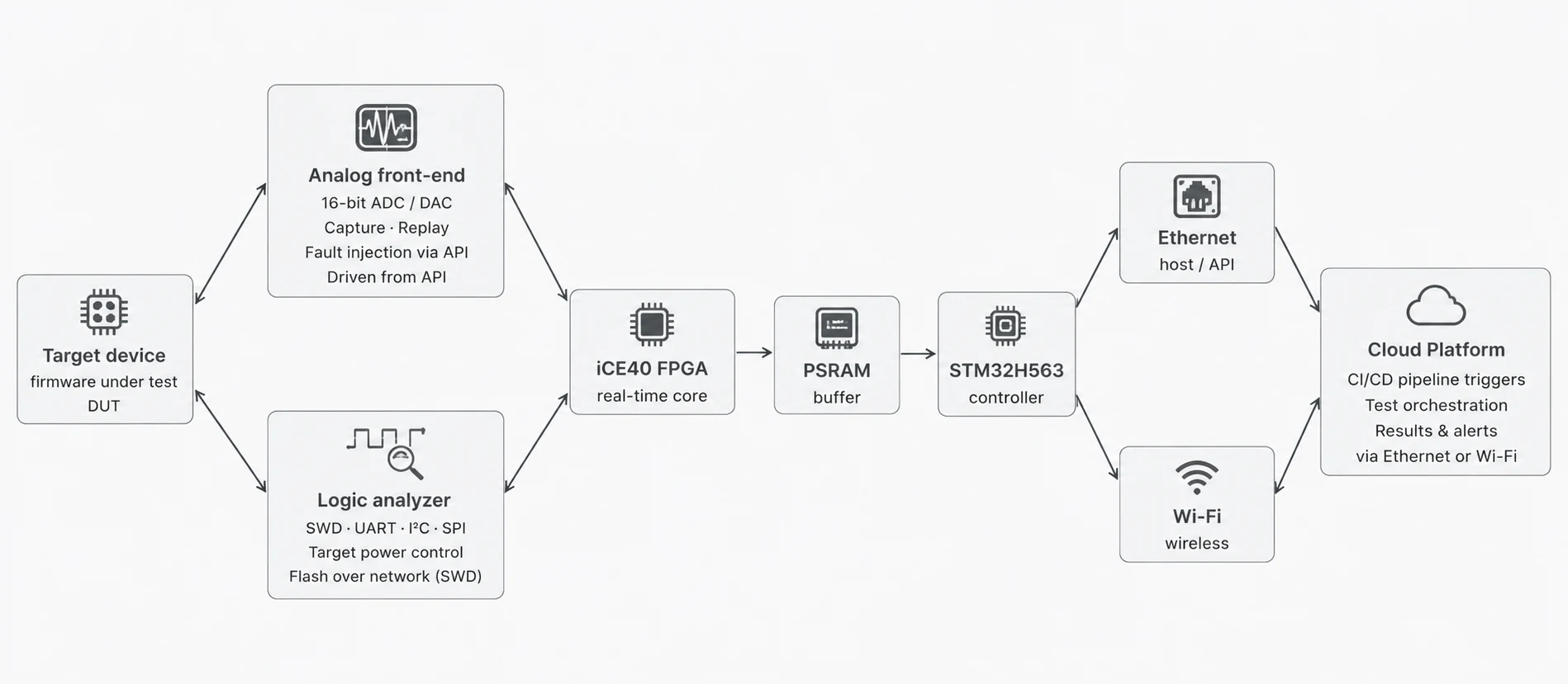
The BenchPod started from a frustration most embedded teams share: you end up with a bench full of equipment that's hard to share, hard to automate, and difficult to use remotely. A power supply, a probe, a logic analyzer, a UART adapter — all tied to one desk. The goal was to fold that pile into a single board you could reach over the network and drive from CI. Getting there took two hardware generations and a long detour through analog design. This is the short version of that story; the full build log lives on Hackaday.
Version 1: the validation board
The first board was about proving the concept cheaply. It paired an RP2350B — picked for its generous GPIO and PIO state machines, which can fake an I2C/SPI sensor without dedicated silicon — with an iCE40UP5K FPGA for the faster work: logic capture, analog streaming, and protocol timing. "An inexpensive way to get real FPGA capability without the board cost getting out of hand." An ESP32-C3 rode along as a deliberately isolated Wi-Fi layer, so the main MCU could stay focused on the test workload.
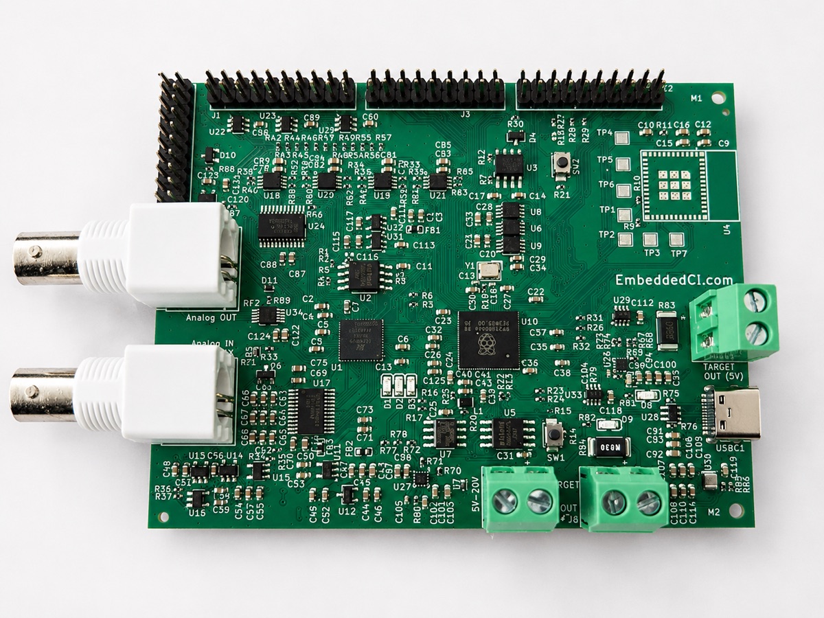
Bring-up taught the usual hard lessons. The analog front-end was basic — 8-bit and bandwidth-limited — with noise and drift that made it useful for digital tricks but not for real measurement. And a mirrored schematic symbol (one stray mouse-click in KiCad) reversed the external flash's pin traces, so the QSPI flash was dead on arrival; v1 ran from SRAM for validation. Annoying, but exactly what a validation board is for: finding these before they matter.
Version 2: a clean redesign
The second generation, finalized in mid-2026, swapped the brain for an STM32H563ZIT6 (144-pin). The deciding factor was networking: native 10/100 Ethernet via an integrated MAC and a LAN8742A PHY, plus six hardware SPI buses and crypto. "It's actually close price-wise, but the RP2350B is short on SPIs if you need Ethernet." With an FPGA already handling the deterministic work, the RP2350's PIO advantage had evaporated — the FPGA had quietly replaced PIO for this use case, which made the trade obvious.
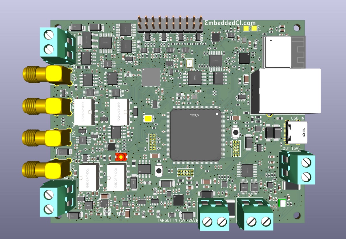
The FPGA stayed, but grew into more: logic capture, ADC/DAC orchestration, and a planned SWD programming state machine. An APS6404L 8 MB QSPI PSRAM gives it room to buffer captures, and a small dedicated flash lets it load its own bitstream.
The analog front-end was the hard part
Most of the redesign's effort went into the analog path, because that's where v1 fell short. "Analog has such a steep learning curve" — a SPICE pass on the old design even turned up missing ADC reference resistors that had to be scratched in by hand.
The v2 input chain is built like instrumentation, not GPIO: a compensated ÷12 attenuator (for a ±30 V range), an OPA810 buffer, a THS4551 fully differential amplifier, into a MCP33131D-10 — a 16-bit, 1 MSPS SAR ADC — against a 4.096 V precision reference. The output side is a 16-bit DAC8551 routed through op-amp buffers and a mux to three ranges (0–5 V, 0–3 V, and a bipolar ±14 V path built from a boost converter and charge pump), plus a separate 4–20 mA current-loop driver for industrial work. BNC gave way to SMA for cleaner signals.
The neat trick is calibration: four reed relays can loop the DAC's output straight back into the ADC's input, so the board checks its own output against its own measurement and corrects for drift — no external gear, no manual step. That self-calibration is what makes recording and replaying real analog signals — and injecting faults on purpose — trustworthy on every CI run.
Power you can cycle from anywhere
Three TPS259470A eFuses switch and protect the target's power rails, so a remote runner can power-cycle a board without anyone touching it — and INA238 monitors report voltage and current per rail. "Being able to turn the target board on and off remotely is more useful than it sounds." Flashing, power cycling, and serial capture all become things a script does, not a person.
Keeping it to one board
What's quietly impressive is that all of this — 144 STM32 pins, a full analog chain crossing a digital one, an FPGA, PSRAM, Wi-Fi, relays — fits the same board outline as v1. The layout strategy: analog on top, power on the bottom, digital threaded between. "RMII is on all sides, SPI is on all sides, so there's no perfect orientation," which forced some creative routing to avoid paying for extra copper layers.
Where it is now
As of late June 2026, v2.0.0 is in production, the schematic and layout are done, and the embeddedci pytest library is on PyPI so you can drive hardware straight from a test. Recent work wired up CMSIS-DAP over TCP for GitHub Actions — tunneled through the EmbeddedCI cloud over a WebSocket, authenticated by device key, no secrets in the workflow. Still ahead: the FPGA-based SWD state machine for on-pod programming and full v2 bring-up. In the maker's own framing, "this is a bring-up board… not production-ready and isn't trying to be."
Want the deep version? The full schematics, photos, part choices, and build logs are documented on the project page. Learn more about the BenchPod on Hackaday →